Waveform Generator
(Project completed: 1990-03-04)
Description
When I was taking Electronics Engineering Technology at George Brown College in the late 80s and early 90s, there was an electronics design contest help by the instructors one year. I don't remember the precise rules, but entrants were to design, build, demonstrate And explain an electronic product of roughly the complexity of a piece of electronics lab equipment - actually, it might have specified lab equipment. The prizes were also lab equipment. Judging was done by a group of electronics instructors.
I designed and built a wafeform generator (also referred to as a signal generator) based around the ICL8038 waveform generator IC. I added output power amplifiers, an output frequency meter and input controls for frequency range, duty cycle, sine wave distortion and separate amplitude and DC offset controls for each wave shape.
Being a poor student at the time, I built the device using almost entirely salvaged parts that I already had on hand. I bought the 8038 chip and etched the circuit board, but everything else was from my lab stock. Some design compromises were made to facilitate this cost saving measure.
One of the judges wanted to disqualify my design because he thought it was tantamount to cheating to use an IC to generate the wave shapes; he expected a signal generator to be done entirely with discrete components. The other judges convinced him otherwise, the main counter-argument being that using an off-the-shelf component to save time and cost is good engineering practice.
In the end, despite multiple amateurish design flaws, I won a prize - an oscilloscope. I don't recall if that was first prize but I think it was.
I still have the device and it still works, though the frequency range switch gang mechanism sticks pretty badly now.
Unfortunately I've lost the original schematic - it might have been kept by the school. The schematics below were reconstructed by inspecting the circuit board, but may contain errors because it's easy to make mistakes when doing this without removing components.
Photos
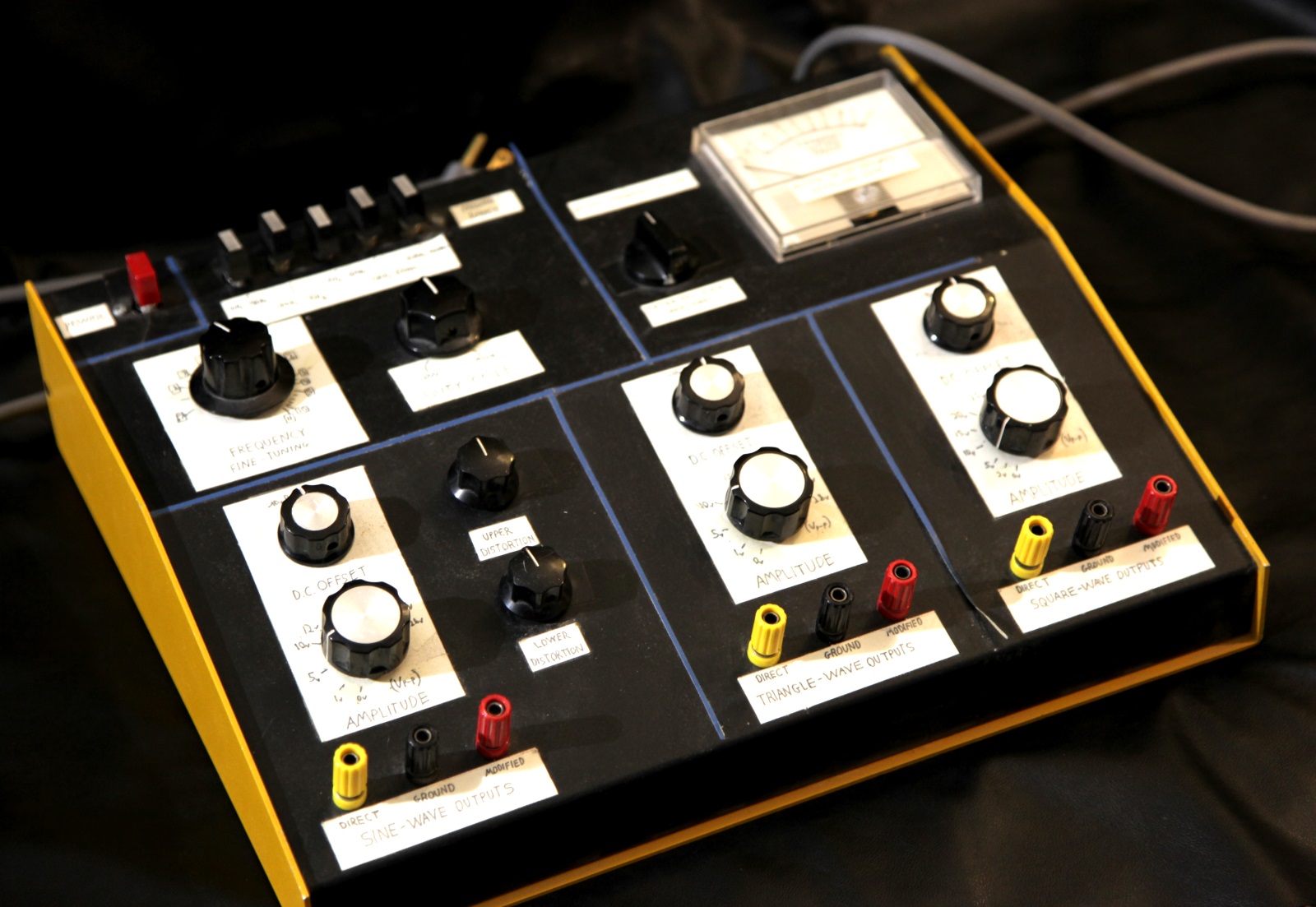
Profile view of the device. Click for full size.
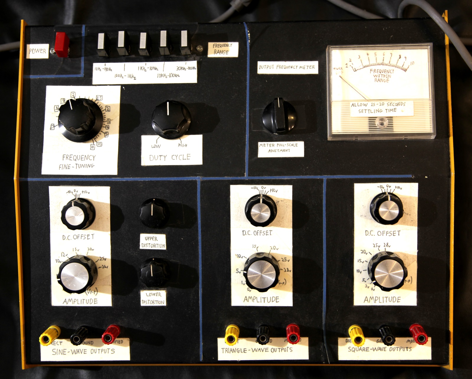
Top view of the control panel. Click for full size.
The above photos show the control panel of the device. The top left section (as outlined with the blue duct tape strips) is for setting the output frequency. The five buttons are ganged to be mutually exclusive and were salvaged from an old stereo system. The first four ranges cover from 10Hz to 100kHz in decades. The fifth range is 30kHz to 300kHz, which is the maximum output frequency of the 8038. The big knob is for fine-tuning the frequency and the small know controls the duty cycle.
The top right section displays the output frequency on an analog meter. The knob is for calibrating the meter.
The three sections in the lower half of the control panel are for the three output signals. From left to right: Sine wave, triangle wave and square wave. In all three the large knob is for controlling the amplitude of the modified output and the smaller knob above it is for adding a DC offset.
The sine wave section has two additional knobs for controlling the distortion of the sine wave. They don't affect the other wave forms. Their operations isn't very intuitive but easy enough to play with until you get a shape you want.
The banana jacks (shown as test points in the schematics) in each output section are for the unmodified output (yellow), ground (black) and modified output (red). The modified output is the one that has the amplitude and DC offset modified by the controls.
Example Outputs
The photos below show some examples of the wide variety of wave shapes that can be made with this device.
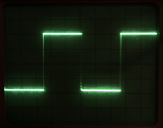
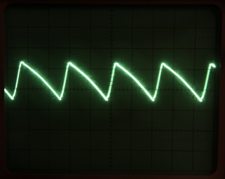
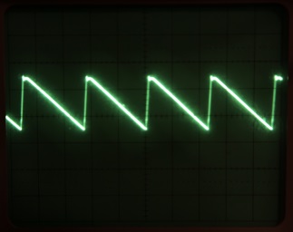
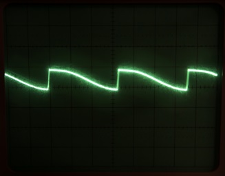

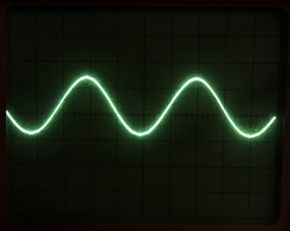
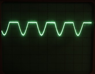
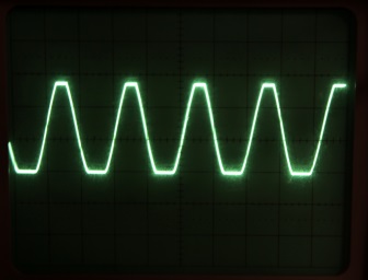
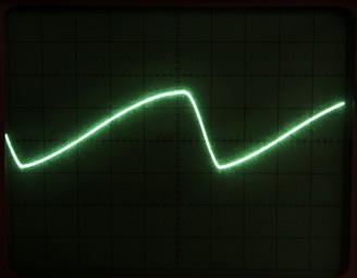
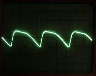
The oscilloscope photos were taken after the device had been on for a few minutes; for some reason all of the outputs have a lot of ringing between the rising and falling portions of each cycle until it has had a few minutes to warm up. It's likely a problem with my design but I never investigated.
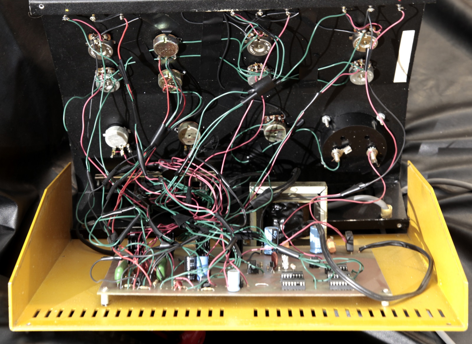
Circuit
Interior of the device. Click for full size.
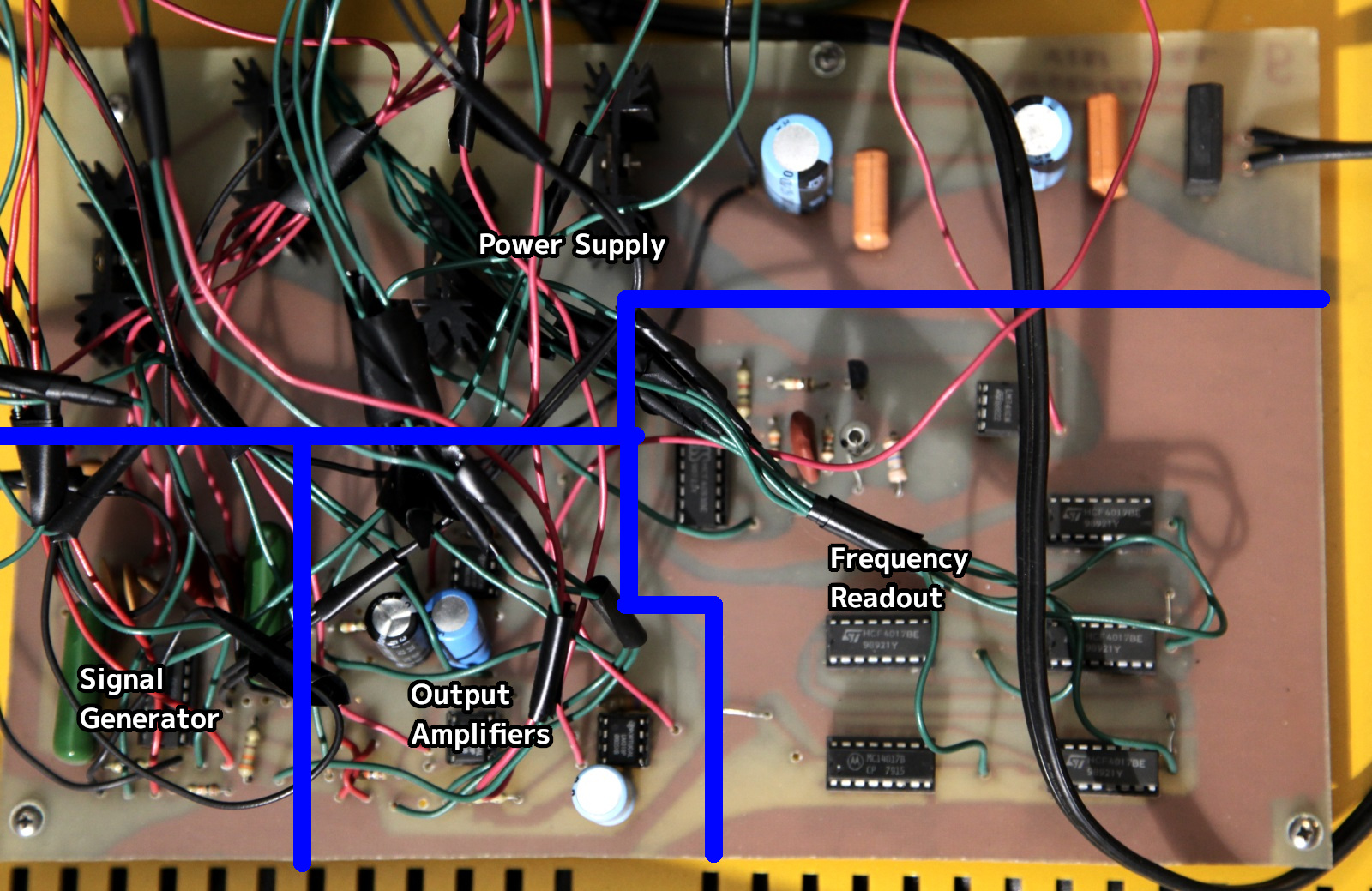
Annotated photo of the top side of the circuit board. Click for full size.
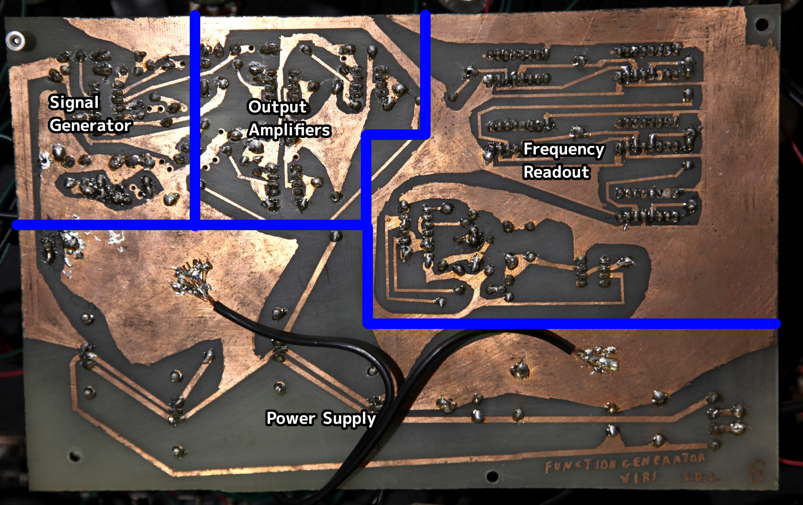
Annotated photo of the trace side of the circuit board. Click for full size.
As you can see in the above photo, the interior of the device is a bit messy. I didn't have access to any decent tools for managing all the wires leading to the control panel, nor any suitable connectors to put on the circuit board.
The frequency readout section takes up a disproportionate amount of the board - it has the most chips and a good share of the discrete components too. The power supply section is also large, but more out of convenience; it let me space out the heat sinks a bit more and put the regulators closer to where their outputs are used.
The sections below describe the four major sections of the circuit in more detail.
Power Supply
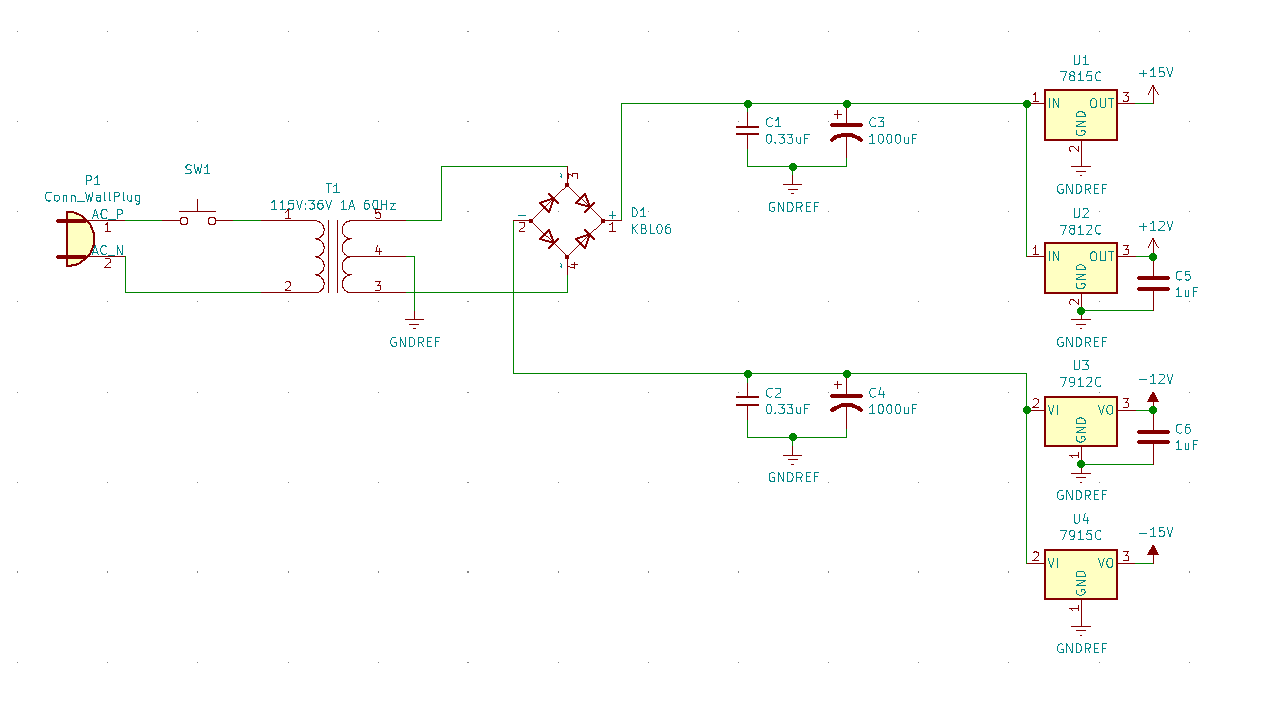
Power supply schematic. Click for full size.
The power supply is pretty straightforward - transformer, full-wave rectifier, smoothing caps and voltage regulators. The +/- 12V supply is needed by some of the chips, and the +/- 15V supply is for the amplified outputs. I could have set the voltage range for the amplified outputs higher than 15V, but I didn't have suitable regulators and transformer on hand.
Signal Generator
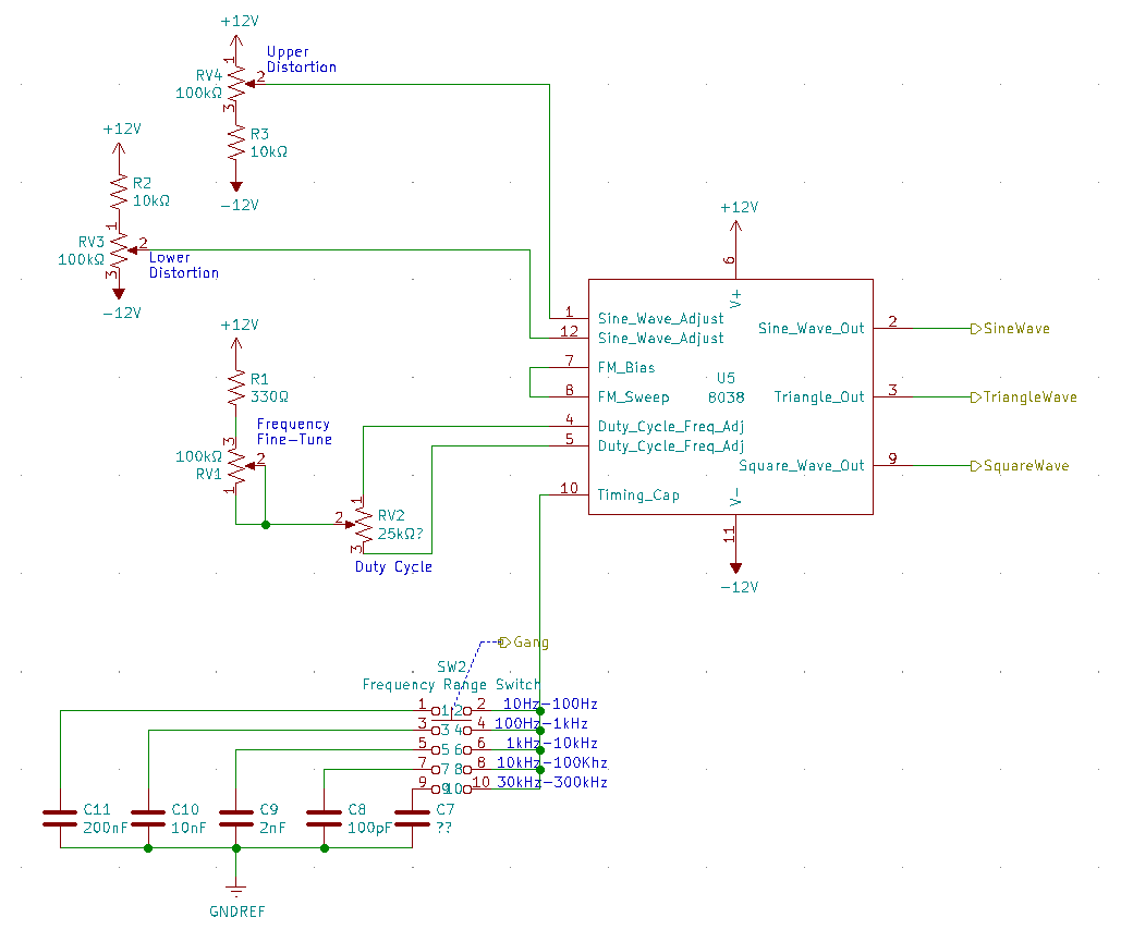
Signal generator schematic. Click for full size.
This circuit was based on a usage example, I think from the 8038 data sheet or from one of those electronics recipe bibles. One mutually-eclusive set of the ganged switches selects the frequency range by selecting different timing capacitors at bottom - note the value of C7 isn't shown because I wasn't able to read it off the component.
The duty cycle and frequency adjustment part of this circuit proved imperfect; the same two inputs of the chip set both - each controls the duration of half of the duty cycle, and the sum controls the frequency. As wired, they don't provide independent control of frequency and duty cycle. I think a more sophisticated physical mechanism or the user of digitally controlled potentiometers could overcome this problem.
Output Amplifiers
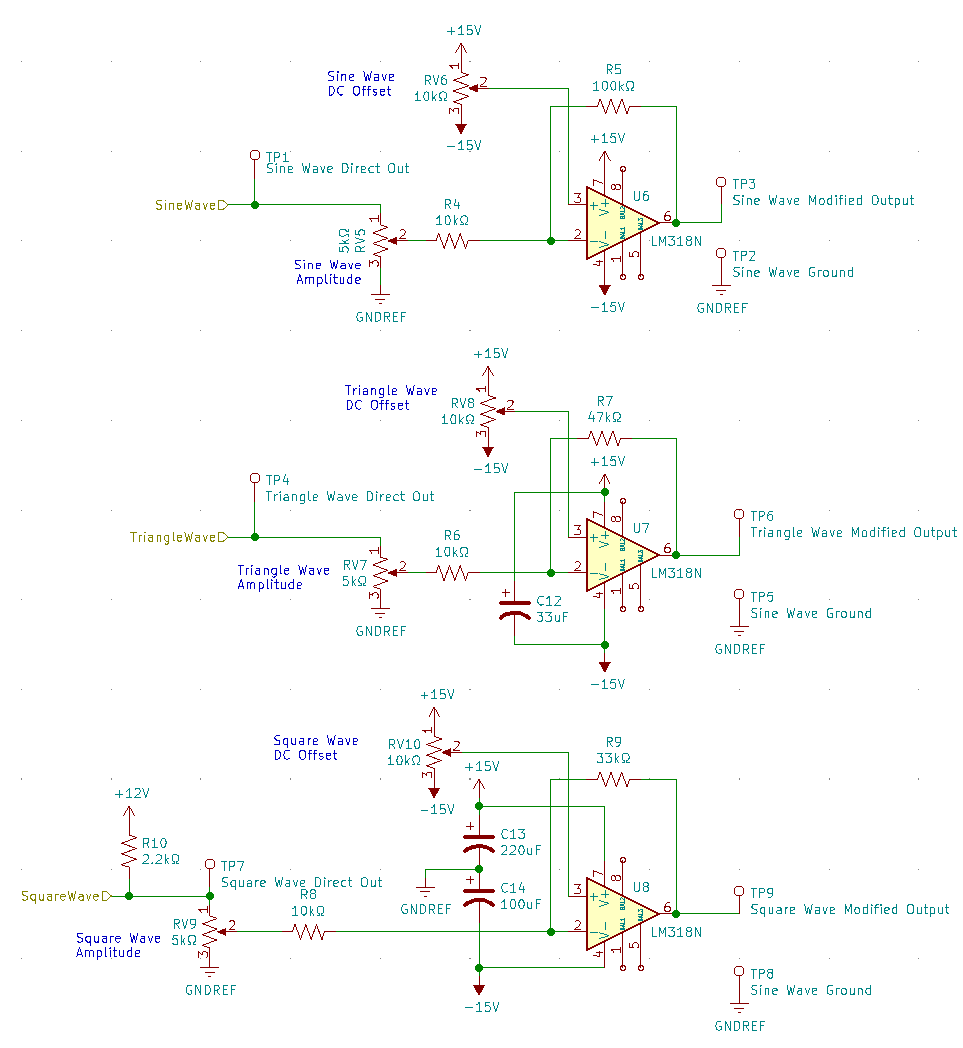
Output amplifiers schematic. Click for full size.
Frequency Readout
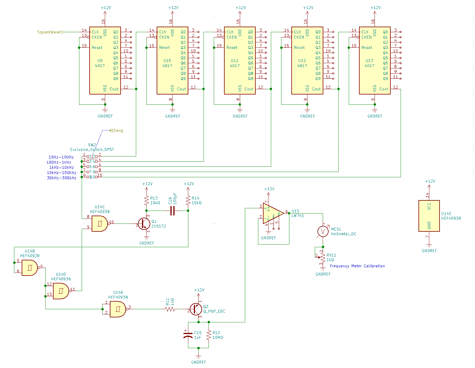
Frequency readout schematic. Click for full size.
Lessons Learned
If I had had the resources and budget at the time I definitely would have used header connectors or some other kind of connector to link the front panel controls to the circuit board to make it possible to disconnect them for repairs. I also might have made the frequency display digital instead of analog.
With the benefit of the things I've learned since, I would use heat-shrink tubing to protect the wire-to-wire solder joings intead of electrician's tape. The tape always eventually lets go and leaves things sticky.